|
|
|
Who's Online
There currently are 6043 guests online. |
|
Categories
|
|
Information
|
|
Featured Product
|
|
|
 |
|
|
There are currently no product reviews.
 ;
nice completed SERVICE MANUAL as the description THANK YOU !!!-
;
Hard to find service manual describing the PLL circuit of the AKAI AP-306.
Thanks to have it available.
;
Gut, sehr gut! It helps me much! I couldn't find this schema nowhere. Good quality
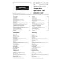
Schematics/Layouts (V15)
System Block Diagram
1880 1880 1805 MHZ 1805 MHZ
NSE�5
187 MHz
71 MHz
13 MHz
RXINP/ RXINN
RX ADC 12bit
I+ modulato Q
r 541.6 kS/S 8kS/S
DLR�3 Supply (MCUGENIO0) AUDIO
UI
Earpiece
58 MHz 116 MHz GSM/PCN Diplex GSM Duplex f/ 2 f 960 935 PCN Rx/Tx MHZ 232 MHz f .. f/4 Summa, Crfu3 Summa Charge. Vref Vcp Vxo Vsyn_1 Vrx_1 Vsyn_2 Vrx_2 Vtx TXIP/ TXIN SYNTH �ENA1 �CLK �DATA TXQP/ TXQN RXC TXC
RX AUDIO DAC 13bit
Headset
SUMMA
116 MHz GSM
CRFU3
Band Select 2067 1992 MHZ .. 464 MHz VHF VCO f/2 UHF VCO 2067 MHz 1942 ..
PCN Tx
Vctcxo Crfu3, lo_buff Rx, Tx, Synth. Crfu3, Rx Summa, VCO�s Summa, Rx Crfu3, Summa, Tx
TxC/AGC DAC10bit
XEar SGnd
mic bias
8kS/S
f f/2 Rx + GSM Tx 16/17
f f/2
slide MIC
XMIC
EXT. RF
Vtx Diplexer
TX AUDIO ADC 13bit
Couplers 915 890
.. .. .. MHZ .. f 1031 MHZ 1006
Headset
232 MHz PCN
TXI DAC 8bit TXQ DAC 8bit AFC DAC 11bit
1.083kS/S
2017 MHZ 1942
PLL LOGIC
64/65
1.083kS/S
COBBA _GJP
st 64 BGA
KEYBOARD PDATA register
Buzzer
Det BIAS PA GSM
116 MHz
AFC
1 kS/S
2
Keyb.� lights slide position
13MHz
232 MHz
3
Vcobba
roller input KEYB.
BIAS
PA PCN
1785 MHZ 1710
VCTCXO RFCLK
Vbb COBBACLK 13MHz COBBA RESET
SERIEL RF/CTR IF
SERIAL AUDIO IF
PCM(3:0)
IMEI� register
DET_FB
SERRFI(3:0)
BAND_SEL IRON NC MCUDA (15:8) ROM1SELX MCUAD (21:0) MCUDA (7:0) MCUWRX MCURDX MCUGENIO3 DSP GEN Out4 DSP GEN Out2 RX Pwr TX Pwr Synth Pwr DSP GEN Out5 DSP GEN Out3 NC NC HOOKDET, HEADDET TXP VCXOPWR BUZZER
LCDRSTX
FrACtrl
Display/Driver Temp.�sense (LCD)
Vpp ctr. ROM (FLASH) 2M*16 SRAM 512k*8
SCU MCU�If
boot rom
CTSI
PUP
MBUS VIBRA
SYSTEM CONNECTOR INTERN VIBRA IR�MODULE TFDU4100
BUSC
API RAM 2kx16 Tone� Generator Sidetone
ACC IF LCD� driver IF
FBUS Rx/Tx ROW(5:0), Col(4:0), LCDCS, ROLLER_A, ROLLER_B, ROLLER_C
RAMSELX
DSP
PCMSIO
UI USER INTERFACE
CS CELLULAR SYSTEM
RSS� Measurement and AGC RX� Filtering ROM 68kx16 RAM 10kx16
8kHz
SNR� Calculation and AFC Phase� Demodu� lation Matched Filter Channel Estimation Symbol Sync. BFI CRC DTX Convol. Encoding Convol. Decoding Inter� leaving Deinter� leaving Bit� Detection De� cryption
COBBA� IF RX RAM TXC RAM TXC Ramp GMSK� modulator TXIQ RAM
MFI UIF
Keyb. IF CCONT IF
GENSCLK GENSDIO SIMCard CLK
CCONT
st 64 BGA SIM IF SIO Mux/ ADC
RSSI EAD BTEMP BSI VBAT ICHAR VCHAR VCXOT LCD� Temp.
5
MCU
DDI DATA DEVICE INTERFACE
SIM CARD READER BATTERY
VIBRA BTEMP BSI
SIM IF MFI FSM
RF
CCONTCSX
DEV DEVICE CONTROL
DSP DSP CONTROL
RX� DTX Speech Decoding HF AEC
8kHz
Voltage Regulators
BB VSIM 3/5 Vref V2V Vcp Vbb V5V VBB VR1 VR1_SW VR2 VR3 VR4 VR5 VR6 VR7 SLEEPCLK, PURX, CCONTINT Vbb Vref
HW HW DRIVERS
LOC LOCALS CONTROL
Speech Encoding VAD
Offset Counter & Comparator FrACtrl TXP
SYSTEM LOGIC
Vxo Vsyn_1 Vrx_1 Vsyn_2
CHAPS SO16
CHARG CHARGER CONTROL
LN LOCAL NETWORK
OS OPERATING SYSTEM
Transmit Control
Transmit�burst every 4.615 ms
Burst Build
En� cryption DSP IO DSP IF Coder
Ram_ bck Vcobba
CharLim
wd
RTC PWM PWM
JTAG
JTAG
Vrx_2 Vtx
MAD2PR1
ti 144 BGA
OSC 32 kHz back�up battery
HD945
Draft
Block Diagram
TEST IF
v. 2.1+ 13 Aug 98
Issue 1 07/99
Page
A�1
|
|
|
> |
|